Two-dimensional (2D) van der Waals heterostructures bring new opportunities to materials physics, electronic and optoelectronic semiconductor device technology. The heterostructures are usually composed of layered materials through weak van der Waals forces, but it faces great challenges when integrated with traditional three-dimensional materials, especially metals. Traditional metal deposition techniques will destroy 2D materials, resulting in interface disorder and defects, which in turn lead to problems such as low carrier injection efficiency and high contact resistance, hindering the observation of new physical phenomena and the development of 2D nanodevice technology. Currently, developing a simple and reliable metal electrode transfer technology that is compatible with the preparation of 2D devices has become a hot topic. In recent years, a strategy based on mechanical transfer of pre-deposited metal contacts has gradually emerged, which achieves an ideal interface and adjustable interface barrier between metal electrodes and 2D materials by maintaining low-energy van der Waals interactions rather than chemical bonds. However, existing mechanical transfer methods still have some problems, such as being limited to specific metals or introducing additional sacrificial layers.
To solve the above problems, Assistant Professor Ou Qingdong and Postdoctoral Fellow Xing Kaijian from Macao Institute of Materials Science and Engineering, Faculty of Innovation Engineering, together with Professor Dong-Chen Qi from Queensland University of Technology, Professor Michael S. Fuhrer of Monash University and an international collaboration team, with Macau University of Science and Technology as the first affiliation, published a research paper titled “Pick-and-Place Transfer of Arbitrary-Metal Electrodes for van der Waals Device Fabrication” in ACS Nano.
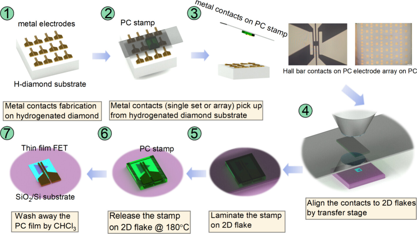
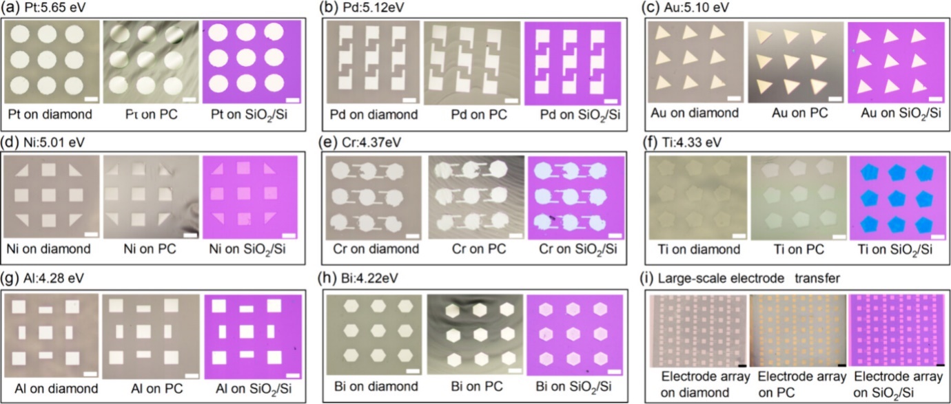
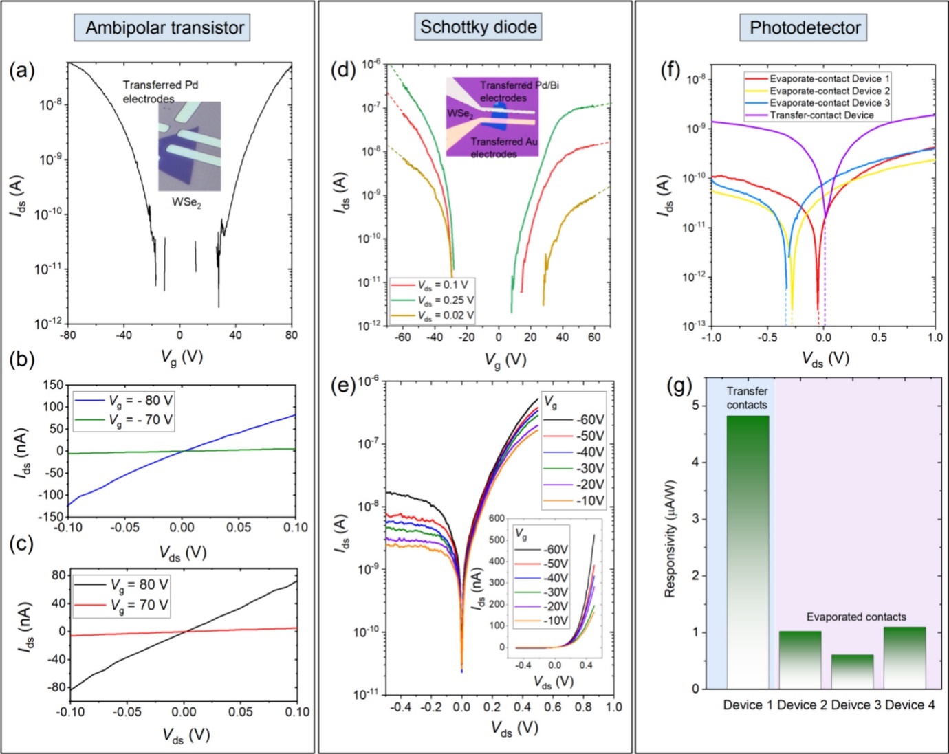
The research team has pioneered a universal pick-and-place transfer technology for arbitrary metal electrodes, which bypasses the use of sacrificial layers in traditional methods. By leveraging the ultra-low adhesion and no dangling bond characteristics of the hydrogenated diamond surface, they achieve efficient stripping and precise transfer of pre-patterned metals to 2D semiconductor materials. This technology successfully achieved the precise transfer and release of 8 different metals, with metal work functions covering 4.22 eV to 5.65 eV. In addition, the hydrogenated diamond substrate can be repeatedly used for transfer without special processing. Finally, through this transfer electrode technology, a variety of functional nanodevices such as bipolar field effect transistors, Schottky barrier diodes, and photodetectors based on 2D transition metal sulfide semiconductors have been constructed. This new technology has the advantages of simplicity, reliability, strong compatibility, and reusability. It provides a new manufacturing method for the preparation of atmospheric environment sensitive 2D material-based devices, and also opens up a way for exploring new physics such as correlated quantum states or topological states.

Figure 1. Schematic diagram of hydrogenated diamond-assisted arbitrary metal electrode transfer for 2D semiconductor device fabrication

Figure 2. Optical microscopic images of metal electrodes with different work functions before and after transfer

Figure 3. Bipolar field effect transistor, Schottky barrier diode and photodetector fabricated by transferred electrodes
Article URL: https://doi.org/10.1021/acsnano.4c13592
First author: Dr. Xing Kaijian from Macau University of Science and Technology, Daniel McEwen and Dr. Yin Yuefeng from Monash University
Corresponding author: Dr. Xing Kaijian and Assistant Professor Ou Qingdong from Macau University of Science and Technology, Professor Dong-Chen Qi from Queensland University of Technology, and Professor Michael S. Fuhrer from Monash University
Kaijian Xing, Daniel McEwen, Yuefeng Yin, Weiyao Zhao, Abdulhakim Bake, David Cortie, Jingying Liu, Thi-Hai-Yen Vu, Yi-Hsun Chen, James Hone, Alastair Stacey, Mark T. Edmonds, Nikhil V. Medhekar, Kenji Watanabe, Takashi Taniguchi, Qingdong Ou, Dong-Chen Qi, and Michael S. Fuhrer,“Pick-and-Place Transfer of Arbitrary-Metal Electrodes for van der Waals Device Fabrication”ACS Nano 2025, DOI: 10.1021/acsnano.4c13592.


